The incredible shrinking solar cell
With lilliputian collectors, almost anything could be sun-powered
The next generation of solar cells will be small. About the size of lint. But the anticipated impact: That’s huge.
Some of these emerging electricity-generating cells could be embedded in windows without obscuring the view. Engineers envision incorporating slightly larger ones into resins that would be molded onto the tops of cars or maybe the roofs of buildings. One team of materials scientists is developing microcells that could be rubber-stamped by the millions onto a yard of fabric. When such cells shrink in size — but not efficiency — it becomes hard to imagine what they couldn’t electrify.
“The idea is to develop ubiquitous solar power,” says Greg Nielson of Sandia National Laboratories in Albuquerque. Foldable and moldable modules crammed full of photovoltaic cells could directly power devices or recharge batteries. “You can imagine putting them onto every surface,” he says. “Your cell phone, laptop, backpack, tent — whatever.”
The U.S. Department of Energy is funding more than a dozen labs to investigate photovoltaic physics “at the nanoscale,” notes Linda Horton, who works in the agency’s Office of Science in Washington, D.C. “Our goal,” she says, “is to understand and improve at a very fundamental level the process by which energy from sunlight is translated into electrical energy.”
Concentrate on this
The real trick to creating useful and affordable lilliputian solar cells is not just shrinking their overall size, but cutting the amount of silicon (or another costly semiconductor) that is needed for them to deliver a watt of power.
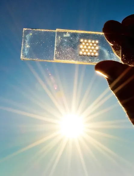
Most photovoltaic devices today are crafted from rigid wafers of costly silicon. At 20 micrometers thick, Sandia’s little cells are less than 10 percent as chunky as the ones used in conventional photovoltaic devices. “And because ours are not just thin, but small laterally, we can do interesting tricks with them optically,” Nielson says. For instance, his group has begun studding minute refractive lenses into glass or plastic plates. Each lens concentrates sunlight onto a solar cell, nearly as small as a pinpoint, that sits directly below.
Silicon is needed only at the focal point of each lens, further diminishing the required quantity to about 1 percent of what’s needed per unit of light-collecting area with commercial photovoltaics. “So silicon is no longer the dominant cost, but a negligible one,” Nielson says.
His group grows thin, pure crystalline silicon, then etch-cuts each wafer into a mass of separate hexagons anywhere from 250 micrometers to 10 millimeters in diameter. “We call them glitter,” says Sandia’s Murat Okandan, and they do sparkle in hues ranging from gold and green to dark purple. Each batch yields uniform and remarkably rugged cells. “We can easily pick them up with a tweezers, and they don’t break,” the electrical engineer says.
The Sandia program, which began in early 2008, is already turning out prototype cells with an energy conversion efficiency of about 15 percent. “And we anticipate getting over 20 percent,” Nielson says. That wouldn’t be far from the best commercial solar cells today, which sport efficiencies somewhat more than 25 percent, Okandan adds.
The small print
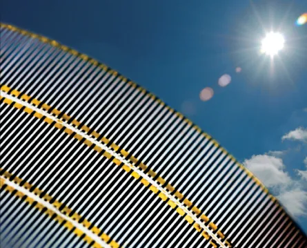
At the University of Illinois at Urbana-Champaign, John Rogers works with even thinner silicon — 10 to 15 micrometers thick — because when it’s slim enough it flexes like a strand of hair. Although he’s testing silicon even thinner than that, the material presents special challenges, he notes, “because even at 10 to 15 micrometers the silicon won’t absorb all of the incident light.” Much passes through.
By backing the cells with a reflective material, however, photons that initially evaded the silicon will bounce back for a second chance at collection. “We found that 15 micrometers is just about the right thickness for that kind of double-pass configuration,” Rogers says. “It will collect about 90 percent of the light.” And the efficiency of these cells is already good, he says, on the order of 12 percent.
The Illinois microcells also rely on concentrators to focus sunlight. Another key to keeping cell costs low, Rogers contends, will be avoiding a need to “pick and place” each cell individually within a module of perhaps legions of others, which is what the integrated circuit industry does today. In the February Energy & Environmental Science, Rogers’ team describes a way to simultaneously lift and transfer thousands of microcells.
After building a block of pure crystalline silicon, the researchers etch out thousands of tiny cells from its surface by cutting around the sides of each one and even underneath. After the etching process is finished, the only thing holding the cells to the starting silicon are tiny anchors of material left at either end of each cell.
The scientists then place a soft piece of slightly tacky rubber onto the batch of cells and press down just hard enough to fracture the anchors. When they lift this rubber pad up, the freed cells come with it.
“We can lift up thousands of these cells at a time and then simply rubber-stamp them down onto a surface” coated with a thin-film adhesive, Rogers says. “Our throughputs correspond to millions of devices per hour — much, much higher than can be achieved with even the most sophisticated tools for doing that [by] pick-and-place.”
Sparse pile
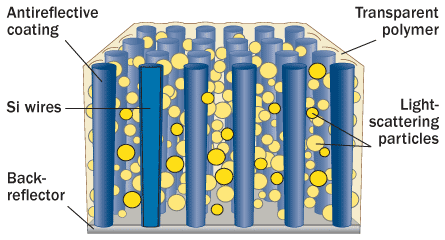
Caltech scientists have upended the silicon elements in their microcells and jettisoned the concentrator. In the April Nature Materials, the team describes a prototype that resembles a sparse carpet of tiny fibers that stretch up toward the light. In the latest designs the fibers are 100 micrometers long and 1 or 2 percent as wide.
Some photons entering the carpet will immediately hit a semiconductor fiber. Many more will miss the wires, which cover only 1 to 5 percent of the carpet’s footprint. But by making the wires effectively long and the carpet’s bottom reflective, photons not initially collected will ricochet repeatedly within the carpet until the silicon collects most of them, explains team leader Harry Atwater.
To protect and hold the fibers, the Caltech scientists pour a liquid akin to clear bathroom caulk (a polymer that solidifies into a pliable plastic) to fill space separating the carpet’s sparse pile.
“We can now peel this composite array of wires and polymer off the starting substrate just as if it were a piece of Scotch tape,” Atwater says. The solar cell — this wire-studded polymer — “has the mechanical properties of a plastic bag,” he notes. “So you can roll it or bend it and the wires won’t break.”
By maximizing photon ricochets within the carpet, the applied physicist explains, “you’re getting the same light absorption as you would from a sheet that’s 100 percent silicon,” but using only 1 percent as much of the pricey material.
Unlike systems that rely on concentrators, which don’t work well on cloudy days, “this kind of cell has equally good absorption for light entering at oblique angles — like when the sun is low in the sky or when light is scattered by clouds.”
Prospects
Although none of the emerging designs are quite ready for prime time, several groups think that products based on their innovations could enter the marketplace in as little as three to five years.
“Right now the solar industry is kind of in a race to bring costs down to $1 per watt,” Nielson says. “From our cost models, it looks like we can get well below that with high-volume production.” But that’s a ways off, he concedes, since his team has only just begun networking individual glitter cells to make coordinated modules.
Atwater has conducted all of his experiments with silicon carpets a few square centimeters in size. “The technology looks promising,” he says, “but you have to ask: Will everything translate when you scale up to very large areas?”