Heart of the Matter: Scanning scope digs deeper into microchips
Princesses may feel peas under huge stacks of mattresses, but semiconductor manufacturers have a much harder time detecting minuscule defects within the crystalline layers of their microchips. So, they have difficulty determining when something goes wrong in the manufacturing process. Now, researchers have developed a noninvasive imaging technique that lets them see deep inside a chip.
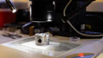
Scanning-probe microscopy, a family of techniques that can portray surfaces in exquisite detail, is routinely used for analyzing chip materials. But defects that are buried more than 5 to 10 nanometers below the surface are “pretty much impossible to see,” says Vinayak P. Dravid, a materials scientist at Northwestern University in Evanston, Ill.
To give depth perception to their scanning-probe microscope system, Dravid and his colleague Gajendra S. Shekhawat rely on acoustic waves. A so-called sample wave travels through a specimen from below and meets another acoustic wave emitted from the microscope’s probe above the sample.
When the sample wave encounters defects, its frequency and amplitude change, and that disturbance is carried into the interference pattern generated by the two waves, explains Dravid. The scanning-probe tip, which also acts as a receiver, “listens to these slight perturbations,” he says. The probe transmits information to a computer, which then depicts the specimen’s interior.
“I think [the technique] opens some really exciting avenues,” says Robert Geer, a materials scientist at the State University of New York at Albany. One challenge now, he notes, is to identify how various material flaws, such as voids and extra atoms, show up in the images.
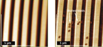
Dravid and Shekhawat, who describe their work in the Oct. 7 Science, have detected gold nanoparticles that they had implanted under a 500-nm polymer layer as a test. They also used the technique to find holes buried in a structure of peaks and valleys that is created as an intermediate step during a chip’s manufacture. Such holes, if undetected, would reduce a chip’s performance, says Dravid.
“It’s the first method I’ve seen to directly image these subsurface voids in an opaque material nondestructively,” says Alain C. Diebold of SEMATECH, a consortium of semiconductor manufacturers. “This kind of tool could have a lot of applications in research and development for the semiconductor industry.”
Along with imaging microelectronic components, Dravid expects his system to be useful in biological research. Unlike other scanning-probe microscopes, the acoustically enhanced system doesn’t require the tip to come in contact with the surface. Therefore, it can be used on “soft” structures, such as cells, says Dravid.