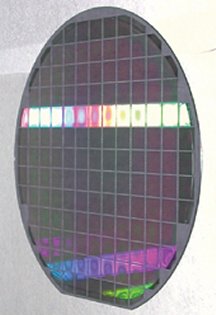
There’s a gleam in electrical engineer Shawn Yu Lin’s eyes these days. It’s a reflection of yellowish light given off by a brightly glowing metallic flake inside a vacuum chamber. Heated to incandescence by an electric current, the metal sliver in Lin’s lab at Sandia National Laboratories in Albuquerque is made of tungsten, as is an ordinary light-bulb filament. But this experimental filament is markedly different from the delicate wires that light up homes and businesses. Electron-microscope imaging reveals the sliver as tiny tungsten rods, each less than one-hundredth the thickness of a human hair, neatly stacked in crisscross layers.
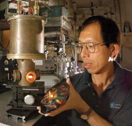

That perforated structure, designed and fabricated by Lin and his coworkers, makes the radiation shining from the rods remarkably intense. What’s more, that intensity lies within an exceptionally narrow band of wavelengths compared with the emissions from ordinary heated tungsten.
This special quality of the emissions, recently recognized for the first time, has raised the prospect of important technological advances based on the new material. Among them may be incandescent lightbulbs many times more efficient than those available today.
The new material is a type of photonic crystal–an orderly, periodic array of rods, pillars, or other structures that interacts with electromagnetic radiation in a special way. Using heated photonic crystals as radiation emitters is a new idea that Lin’s group is the first to try, says Eli Yablonovitch of the University of California, Los Angeles, a founder of the photonic-crystal field. “It’s very original,” he says.
The emissions’ characteristics may also have repercussions in fundamental physics. They apparently contravene the century-old Planck’s radiation law, one of the pillars of scientific understanding of heat and radiation. Consequently, many scientists have challenged the new findings.
Some of the explanation for the unusual findings must lie in the novel way in which the tungsten microstructure responds to certain wavelengths of light, Lin and his team say. Still, they admit that they don’t yet fully grasp what’s going on in their invention.
Back to the source
A photonic crystal allows radiation of certain wavelengths to enter its structure but blocks others. The size of the spacing between lattice elements–in this case, the tungsten rods–corresponds roughly to the wavelength of accepted radiation.
Cavities or channels built into a photonic structure can permit the passage of radiation that wouldn’t penetrate the unaltered crystal (SN: 10/24/98, p. 271). Researchers can therefore create devices that steer radiation through the crystal in a controlled manner, making possible light-manipulating components such as waveguides, prismlike light splitters, and lasers.
Not far off, say the technology’s developers, are photonic microcircuits that process light beams the way today’s microelectronics chips process electric currents. Among many potential advantages, such light-based circuits should run faster and consume less power than microelectronic ones do.
One goal for photonics is to build a tiny light source onto such chips to provide the photon currents needed. Developers of such sources focus on infrared light because it’s already used in fiber-optic telecommunications. Many teams have investigated electronic means for triggering infrared light emissions.
In the late 1990s, however, Lin and his colleagues conceived of heating photonic crystals to generate radiation for photonic chips. Because thermal radiation typically is smeared over a wide range of wavelengths, it’s not naturally suited for the job. The scientists speculated that photonic crystals, when heating, would create narrow bands of emission instead of the usual broad ones.
Metal muddle
In the late 1980s, pioneers of photonic crystals demonstrated the concept using centimeter-scale metal structures to guide long-wavelength radiation such as microwaves. However, metals usually absorb rather than reflect the shorter wavelengths of infrared and visible light that are required for photonic circuits. So, photonic crystals are now typically made of insulating or semiconducting materials, such as titanium oxide, silicon dioxide, silicon, or gallium arsenide.
As Lin and his colleagues began to work with heated crystals, they were well aware of metals’ unwelcome absorption of light. In the team’s first test of thermal excitation, they reported that a photonic crystal of crisscross silicon rods, heated to 137C, emitted strongly at wavelengths shorter than 10 micrometers (m) but showed much less emission at longer wavelengths. The findings were published in 2000.
Lin’s team turned to tungsten after considering it for another project. Sandia scientists were developing electric generators powered by radiant heat, as from a furnace, falling onto thermophotovoltaic (TPV) cells. As solar cells convert sunlight to electricity, TPV cells convert infrared radiation into electricity. TPV generators promise to be efficient, quiet, and durable because they have no moving parts. A major difficulty with that concept has been to pack the intense radiation from a heat source into the band of wavelengths at which TPV cells respond.
For the Sandia TPV project, Lin and his collaborators were contemplating fabricating thin barriers of tungsten. Besides having an extremely high melting point, above 3,400C, tungsten absorbs thermal radiation at long wavelengths and reemits it at the short wavelengths suitable for TPV cells.
Theoretical results published by Ihab F. El-Kady and his colleagues at Ames National Laboratory and Iowa State University at Ames had suggested that certain metals might be valuable for photonic crystals after all.
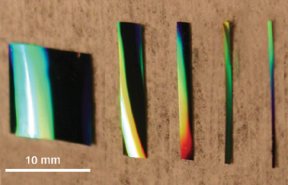
Despite his skepticism of the Ames calculations, Lin decided to try a long shot. His Sandia colleague James G. Fleming proposed a way to use the silicon crystal as a template to make an identical structure in tungsten. When that succeeded, Lin’s group suddenly found themselves in possession of a material unlike anything previously available–a metallic photonic crystal that operates at optical wavelengths.
What’s more, unlike fragile silicon photonic crystals, the material was tough enough to be clamped between electrodes, as a lightbulb filament is.
Over the top
The first optical tests of this new type of metallic microstructure confirmed its photonic properties. In the May 2, 2002 Nature Lin, Fleming, El-Kady, and other Sandia and Ames researchers reported that the material rejected an exceptionally broad range of infrared wavelengths (SN: 5/25/02, p. 334: Available to subscribers at Tiny tungsten beams lord over light). They were startled, however, to find that the crystal absorbed dozens of times more radiation at relatively short infrared wavelengths than did an ordinary tungsten film.
That was a most welcome surprise. A material that absorbs strongly at a specific wavelength when cool will emit strongly at that same wavelength when heated. The unusual absorption of the tungsten photonic crystals signified that they could probably be engineered to emit intensely at the infrared wavelengths desired for photonics and TPV.
Even better, when the team measured the emissions, they were up to tenfold the amount that traditional physics seemed to permit.
Given these extraordinary emission data and because patents were in the works, the researchers kept their findings under wraps. Under orders from Sandia’s management, “we held [the results] for a year without talking,” Lin says. “We worked the majority of last year to confirm and confirm and confirm,” he recalls.
This June and August, U.S. patents were awarded for TPV and incandescent-light applications of the new material. Further patents are pending, Lin says. In the July 14 and July 28 Applied Physics Letters, the researchers unveiled their emission data.
To date, the group has built and studied about 100 tungsten photonic-crystal samples. The most recent version of the tungsten microstructure concentrates its emissions in a band around 1.5 m, an infrared wavelength suitable for driving TPV cells.
Such photonic crystals could outperform other schemes for powering TPV cells, says thermophotovoltaic pioneer Lewis Fraas of JX Crystals in Issaquah, Wash. On the other hand, the crystals would probably be far more expensive to make than typical components for the still-experimental TPV systems are, he adds.
The 1.5-m wavelength is also on target for photonics because that wavelength is widely used in today’s fiber optics networks. However, to drive circuits, the thermal emissions would have to be converted into single-wavelength beams that have light waves moving in lockstep, as laser beams do.
Lin says his group plans to develop tungsten photonic crystals that include, on a single microchip, both a heated region that emits infrared radiation and another region that converts those thermal emissions into laserlike beams for driving telecommunications networks. Today’s radiation sources in telecommunications are “typically as big as a shoebox . . . . Ours [will be] on the centimeter scale,” Lin says.
The photonic crystals’ remarkable funneling of energy to short wavelengths suggests another potential use: as filaments for extraordinarily energy-efficient incandescent lightbulbs. Today’s bulbs convert typically about 8 percent of their electrical energy into visible light. The rest of the energy goes to waste as infrared, or heat, radiation. That’s why lighted bulbs are too hot to handle, notes El-Kady, now at Sandia labs.
A newer technology that uses light-emitting diodes, or LEDs, in car blinkers, traffic stoplights, and other types of lamps attains up to 25 percent electricity-to-optical energy efficiency, Lin says.
In contrast, he estimates that bulbs with photonic-crystal filaments might convert as much as 60 percent of their power to visible-light output. In other words, 6-, 9-, and 15-watt photonic-crystal bulbs would produce more light than today’s 40-, 60-, and 100-watt bulbs do.
The tungsten slivers that Lin tests in his lab radiate only weakly in the visible spectrum. To improve those emissions, the dimensions of the microstructures would have to shrink by a factor of 15, until the rods were only about 1,000 atoms wide. That would be difficult, but it should be feasible in the near future with microcircuit fabrication techniques, Lin says.
His team already uses such techniques to build its microstructures but would need to get help from a chip-making firm to get down to such tiny dimensions, he says.
However, Lin and his colleagues face another, possibly more formidable, obstacle. At visible, rather than infrared, wavelengths, light absorption by the tungsten shoots way up, preventing emissions.
“Tungsten will not work. Its limit is 1.5 m–that’s it. But it proved the principle for us,” El-Kady says.
Now, a different material must be found. On a supercomputer, El-Kady is simulating the behavior of various metal alloys. Besides having the right optical characteristics, the new metal must be strong, able to withstand high temperatures, and easily deposited from a vapor to form the microstructure.
Beyond the law
German physicist Max Planck derived his radiation law in 1900. For any given temperature and wavelength, it specifies exactly how much radiation an idealized thermal source known as a black body will emit. Because a black body is considered the most efficient heat emitter possible, there should be no going beyond the emissions predicted by Planck’s law.
The law applies to all heated solids, El-Kady explains, but not to fluorescent lights, for instance, because their radiation does not arise from the vibrations of heated atoms.
Lin’s photonic crystal, energized by contact with a hot surface, is clearly a thermal source. But from an experiment on one photonic crystal, the Sandia team reports that in the band of wavelengths with the most intense emissions, the heated material yields three times as much infrared radiation as Planck’s law permits. Those findings are scheduled to appear in the Oct. 15 Optics Letters.
“Anytime you’ve broken through a fundamental law of physics, it’s certainly very interesting,” El-Kady says. “We may need to modify Planck’s law to account for effects like this.”
Lin offers an explanation for one way in which the tungsten crystal differs from other heated solids. Photons with wavelengths forbidden in the tungsten crystal either can’t be made or can’t escape the microstructure, he says. Consequently, a photonic crystal measured to have the same temperature, and therefore comparable energy, as a black body has to shed more energy as photons at allowed wavelengths.
Whether the photonic crystal’s behavior challenges physicists’ understanding of heat and light in a more basic way remains to be seen.
Lin proposes a new phenomenon in which photons having wavelengths just outside a crystal’s forbidden band cling to the metal lattice. “It’s like you put honey through the lattice and it stays there a long time,” Lin says. Those photons linger in the crystal before being emitted, so intensity builds up in that so-called band edge.
The photonic crystal may not be merely shunting energy from long to short wavelengths. It might also be emitting more energy across the electromagnetic spectrum than Planck’s law deems possible. Some of the team’s data indicate that this is probably the case, Lin says.
Not everyone believes the Sandia results. “I do not see how they could possibly exceed the black body limit,” comments John B. Pendry, a theoretical physicist at the Imperial College of London. He suggests that Lin and his colleagues may have erred when processing their measurements.
Some other scientists accept the work as valid, however. “The numbers are believable,” remarks Jonathan P. Dowling of NASA’s Jet Propulsion Laboratory in Pasadena, Calif. He’s now applying the same approach to solar cells. Adds Dowling, “I think highly efficient lightbulbs and solar cells far more efficient than anybody could have imagined, are a real possibility now.”
****************
If you have a comment on this article that you would like considered for publication in Science News, send it to editors@sciencenews.org. Please include your name and location.
To subscribe to Science News (print), go to https://www.kable.com/pub/scnw/
subServices.asp.
To sign up for the free weekly e-LETTER from Science News, go to http://www.sciencenews.org/subscribe_form.asp.