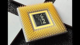
Hungry for details, dozens of microcircuit specialists surrounded Tahir Ghani after his talk last December at an annual microelectronics conference in Washington, D.C. Ghani, a senior-level engineer with the chip giant Intel in Hillsboro, Ore., had sketchily revealed two new types of transistors that his company was getting ready to use in its Pentium microprocessors and Centrino chips. After his talk, Ghani remained cagey. After all, his inquisitors were from IBM, Taiwan Semiconductor Manufacturing Company, NEC, and other rival chip makers. All these companies are confronted by the same daunting challenge: to maintain the swift pace of miniaturization even while their mainstay manufacturing methods are reaching their limits.
For decades, chip manufacturers have made transistors faster by making them smaller. Lately, however, this approach has begun to unravel.
“We’ve now reached the point at which transistors are so small that our ability to keep shrinking them is facing some challenges,” says Jeffrey Welser of IBM Microelectronics Semiconductor Research and Development Center in Hopewell Junction, N.Y. “When we make them smaller, they’re not automatically faster anymore.”
To maintain the furious pace of innovation that’s been the industry norm for decades, component designers such as Ghani and his rivals are now tampering with the very architecture of the silicon crystals from which transistors are made.
“This is a seminal change for the industry,” says physicist Bernard S. Meyerson of IBM’s Technology Group in Hopewell Junction.
Although many microelectronics companies have been experimenting for years with distorting silicon crystals in this way, Ghani at his December talk at the IEEE International Electron Devices Meeting revealed for the first time that the world’s leading seller of chips had actually begun incorporating the deformed material into its products. Meanwhile, many other microcircuit makers have either quietly introduced similarly strained crystals into their chips or are planning to make that move.
“However it is induced, crystal strain is becoming more and more attractive as a means for getting better performance” from a microchip, says Judy L. Hoyt of the Massachusetts Institute of Technology (MIT).
Diminishing returns
The microelectronics revolution is built on silicon. Since the early 1980s, one family of silicon-based transistors, made via a technology known in long form as complementary metal-oxide semiconductor and more often by its acronym CMOS (pronounced SEE-moss), has served as the main building block of that revolution.
These workhorse transistors use an electric field to control a flow of either negatively or positively charged particles. That’s why engineers also describe the devices as field-effect transistors.
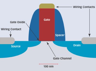
The field encourages or chokes off current in a narrow strip, called the gate channel, that spans the device’s so-called source and drain regions. This on-off switching capacity is what produces the 0s and 1s that make up electronic language.
A thin layer of electrically insulating material, usually silicon dioxide with some nitrogen mixed in, coats the channel and is itself topped by a block of metal-enriched silicon called the gate, which supplies the current-controlling electric field. Today, all of these parts occupy an area that would fit easily in a red blood cell.
One more detail: Depending on the types of material used, chip makers can produce N-type and P-type transistors on a CMOS chip. In N-type transistors, negative charges move between the source and drain. In P-type, it’s positive charges that move. The complementary arrangement on a chip puts the C in CMOS.
The wild success of miniaturization in electronics has owed largely to how conveniently CMOS transistors scale down. Shrinking the transistor primarily entails shortening its gate channel, which means that charged particles have a shorter path to follow between the device’s source and drain. As a result, the operating speed of the transistor has jumped about 20 percent with each new chip generation.
Those in the trenches at chip factories are quick to say that better transistor performance has always taken more than merely shortening gate length. As transistors shrink, for example, the maximum current the transistor can accommodate also declines. Unless that is compensated for, the smaller currents would slow down the entire network of transistors that sum into, say, a microprocessor. The solution to date has been to thin out the insulating oxide layer between the gate and the channel, a measure that strengthens the gate’s field and brings the transistor’s maximum current back up to the desired value.
Recently, however, those gate oxides have become so thin that they permit current to leak, producing what scientists call “off current.” That’s a problem, so some chip makers are seeking alternative materials, but none has yet found one that works as conveniently as silicon dioxide (SN: 3/25/00, p. 204: Looking for Mr. Goodoxide).
Current leakage wastes power, makes chips run hot, and can obscure the difference between a transistor’s on and off states—that is, garble the digital language. For these reasons, Meyerson says, manufacturers can no longer thin down available oxides as much as they used to.
Even the gate channels themselves are now so short that worrisome amounts of current leak from source to drain. “That means we have to be less aggressive in how we scale [transistors] because we need to control that off current,” Welser says. “That’s the major problem the industry faces.”
Not ones to give in to daunting technical challenges, chip makers are turning to an entirely different strategy to keep the combined trends of ever-smaller transistors and ever more performance in lockstep. It’s called strain engineering.
In the semiconductor world until recently, silicon strain was a phenomenon to be shunned. It conjured variations in a silicon crystal, which is anathema to manufacturers that depend on uniformity within the silicon to produce chips with millions upon millions of predictable and reliable transistors. The industry’s approach to strain in silicon crystals was “trying to get rid of it,” recalls Jon Candelaria of Motorola Physical Science Research Labs in Tempe, Ariz.
More than a decade ago, however, a handful of researchers in Europe and the United States—including Meyerson, Hoyt, and MIT’s Eugene A. Fitzgerald, then at Bell Labs in Murray Hill, N.J.—began investigating an arcane bit of physics that underlies strain engineering: Putting a strain on a semiconductor crystal alters the speed at which charges move through that crystal. In 1992, Welser, then a graduate student, and other researchers led by Hoyt, who was then at Stanford University, demonstrated that controlled strain could result in up to a doubling of speed in manufacturable CMOS-type transistors. Even so, no company raced to incorporate the advance into its products, Hoyt recalls.
“More or less, the reason people didn’t jump on it right away is that there was plenty of performance [still] to be gained from scaling” transistors down, she says.
Stretch and squeeze
Chip makers typically create strains in crystalline silicon by applying layers of other materials to physically elongate or compress bonds between the crystal’s atoms.
Not much of either effect is needed for a payoff, notes Dennis D. Buss of Texas Instruments in Dallas. “One percent strain is a huge strain,” he says, and it’s enough to yield a 5 to 20 percent increase in transistor speed.
Strain makes CMOS transistors work better by enabling electrical charges, such as electrons, to pass more easily through the silicon lattice of the gate channel. When the silicon-crystal lattice is undistorted, it offers obstacles to an electron the way a wrinkled bedsheet impedes a rolling marble, Meyerson suggests. From the perspective of quantum mechanics, the wrinkles represent energy variations that impede an electron’s motion. “Now, pull the four corners so the wrinkles vanish,” Meyerson says. That’s strain, and it provides the electrons with a smoother pathway.
Strain influences each type of electrical charges in CMOS transistors differently. Tensile strain, in which the interatomic distances in the silicon crystal are stretched, typically increases the mobility of electrons, making N-type transistors faster. But tensile strain may not benefit P-type devices as much, and it may even slow them down. Compressive strain, in which those interatomic distances are shortened, produces essentially the opposite effects.
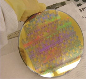
Microelectronics manufacturers create hundreds to thousands of chips simultaneously on large, thin wafers of silicon. Until recently, strain specialists have focused on what they refer to as biaxial strain, created by growing high-quality layers of strained material across entire wafers.
To fabricate that extensive coating, engineers typically first deposit onto an existing silicon wafer a layer of an alloy of silicon and germanium—a semiconductor with properties much like those of silicon. In general, the germanium spaces the silicon atoms farther apart than they are in a layer of pure silicon.
That layer alone wasn’t enough to create the kind of strain that engineers wanted for CMOS transistors, but they found that, if the layer was thin, they could use it to make very fast versions of another transistor type. About 5 years ago, this means of creating strain became part and parcel of heterojunction bipolar transistors, which are in high-frequency circuitry of cell phones and other devices (SN: 1/10/04, p. 21: Available to subscribers at Flashy Transistors: Electronic workhorses also shed light). Says Welser: “That was a very important breakthrough.”
To make the biaxial strain approach work for CMOS transistors requires another wafer layer. On top of a thick silicon-germanium layer goes a thin film of silicon. As its atoms settle onto the alloy layer, they follow the expanded pattern of the underlying layer and forge stretched bonds between each other.
Because of the conflicting effects that strain has on N-type and P-type transistors, this whole-wafer approach of building strain into silicon typically improves the performance of one transistor type more than that of the other. That disparity has held back the commercial introduction of biaxial strain.
In the meantime, another approach to strain engineering has sprinted past the biaxial one. During the past few years, engineers including Ghani and his colleagues have devised ways to selectively strain parts of individual transistors. Using this local effect—known as uniaxial strain—engineers can impose either tensile or compressive strain on both N-type and P-type transistors on the same chip. That means they can use silicon strain to make CMOS circuitry perform better as a whole.
Strain specialists say they expect biaxial strain to soon enter commercial production as well. Combining it with uniaxial strain will enable chip makers to compensate for the uneven effect that whole-wafer strain has on the different types of CMOS components. What’s more, biaxial strain offers some advantages, such as uniformity of strain for all transistors, that uniaxial strain doesn’t provide.
7th inning stretch
Strained silicon has become ready for the production line at just the right time. Miniaturization is petering out and no other approach is ready to use yet.
It’s not that the engineers aren’t looking closely at carbon nanotubes (SN: 11/22/03, p. 324: Available to subscribers at No Assembly Required: DNA brings carbon nanotube circuits in line), semiconductor nanowires (SN: 1/3/04, p. 6: Available to subscribers at Gene Screen: Ultrasensitive nanowires catch mutations), or individual organic molecules (SN: 9/20/03, p. 182: Available to subscribers at Molecular Memory: Carbon-nanotube device stores data in molecules) as potential means for shrinking electronics down to even a few thousandths the size of today’s smallest. But it will take years before any of those exotic options is ready for wide use, microelectronics specialists say.
The big question, notes Robert Guernsey of IBM Research in Yorktown Heights, N.Y., is, “How do you keep going right now?” Although strain engineering is not the only answer, it’s one that’s good to go.
In his December 2003 talk in Washington, D.C., Intel’s Ghani described two different manufacturing approaches using uniaxial strain. Those techniques yielded transistors with about 15 to 20 percent higher speeds at only a 2 percent increase in manufacturing cost, he reported.
Intel’s key advance was “to use not one method, but two different methods at the same time,” Candelaria says.
To strain N-type transistors, the Intel designers added a thick layer of silicon nitride, a material already commonly used in microchip fabrication. When deposited on top of the gate channel, the material created tensile stress in the underlying silicon, thereby speeding up electron mobility there.
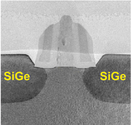
For P-type transistors, the team came at the problem from a different angle. Instead of adding a compressed layer above or below the gate channel to directly induce compression in the channel itself, Ghani and his colleagues replaced the silicon in the source and drain with silicon-germanium. Because silicon-germanium’s lattice is slightly larger than that of the surrounding silicon, this addition pushes on the gate channel from both sides, compressing it.
That squeeze tactic wouldn’t have worked even a couple of chip generations ago, Candelaria says. That’s because gate channels then were too long, and the pressure from such silicon-germanium pincers wouldn’t have penetrated far enough into the channel. In other words, the overall transistor structure finally has shrunk enough that this strain-inducing technique can work, he says.
Ghani’s recent revelation that Intel had begun using strain engineering in its CMOS production lines probably is only a harbinger of things to come throughout the industry.
At the December meeting, for example, several teams reported combining strained silicon with other performance-enhancing innovations in chip architecture and processing that can be implemented now or very soon. Other researchers looking further into the future are exploring replacing silicon in chips with more naturally conductive, siliconlike materials—such as silicon-germanium or pure germanium—and then straining those materials to boost current.
“Because of the progress in the past year or so,” says Candelaria, “people [in the chip industry] are much more believers that this strain is good—that it can be controlled and useful and is not something to be afraid of.”


