Double-laser approach makes one thin line
Erasing and stenciling offers new approach for nanolithography
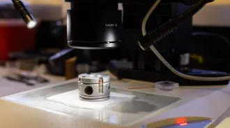
Michelangelo couldn’t have chiseled David’s features with the edge of a backhoe. But just such a challenge faces scientists working in the infinitesimally small world of nanolithography, the ultratiny writing used to make computer chips, solar cells and other devices. Now three reports, published online April 9 in Science, introduce new methods to erase and stencil patterns, putting a finer point on the tools used to sculpt and write in the incredibly shrinking nanoworld.
The research “could spawn all kinds of interesting ideas and new approaches,” comments Greg Wallraff of the IBM Almaden Research Center in San Jose, Calif. “This is really interesting science.”
Current nanolithography techniques use ultraviolet light to etch patterns and images that can be used, for example, to inscribe circuitry on computer chips. Nanolithography is a precise form of photolithography, which shares many fundamentals with regular photography — light is projected through a lens onto a material that reacts upon exposure. For crafting tiny objects or masks used for imprinting circuitry, the material is often a liquid compound called a monomer, which turns into a hardened, repeating version of itself, a polymer, when exposed to light.
Progress has been made in using smaller and smaller wavelengths of light to create the printed patterns, but now that approach is limited in part because of how light behaves at such short wavelengths. And these techniques also require enormous, expensive lenses.
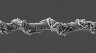
Robert McLeod of the University of Colorado at Boulder and his colleagues decided instead to use two beams of light at the same time — one acting as the ink, the other as an eraser.
Fiddling with the chemistry of the initial light-sensitive materials made the new approach possible. The scientists added two special ingredients, an initiator that reacts with blue light and an inhibitor that reacts with UV light. When the scientists project the blue light through the lens onto the monomer, the liquid absorbs the light and releases radicals that are hungry to bond. And bond they do, linking to other monomers and creating a solid polymer wherever the blue light hits.
The UV light then acts as the eraser, the team reports in Science.
“Imagine trying to draw a very fine line with a thick marker,” says McLeod. “We can make that thick line thinner if we have an eraser.”Surrounding the dot created by the blue light, the scientists shone UV light, which reacts with the chemical inhibitor in the liquid monomer. This process also generates radicals, but these snatch up other nearby radicals preventing polymerization. So the scientists can get a very fine line with the blue light by sweeping the periphery with UV light.
John Fourkas of the University of Maryland in College Park and colleagues report a similar approach: An activating laser beam gets polymerization going, and a de-activating beam keeps the polymerization contained.
“You know that light they shine on your composite fillings at the dentist?” Fourkas says. “Imagine if you could stick a second light on it to control where it is hardening.”
Sculpting with light may allow these researchers to craft tiny gears for tiny machines or finely detailed masks for controlling where light hits a material. Another area of promise is crafting better solar cells, says Rajesh Menon of the Massachusetts Institute of Technology in Cambridge.
In a third paper, Menon and colleagues describe another photolithography technique, one that also uses two different wavelengths of light. But in this case, the researchers blocked light instead of erasing it.
The researchers placed light-sensitive film over the material that they wanted to pattern. Upon exposure to UV light, the film becomes transparent, allowing the scientists to “cut” a window wherever one is desired, creating a stencil at will, through which they can shine light of another wavelength to etch the material beneath.
The approach isn’t only applicable to patterning, Menon says. It would also allow the development of microscopes that would peer into the nanoscale so that biologists could image the behavior of single molecules in cells.
“In my view, this is just the tip of the iceberg,” he says.
The new research probably won’t revolutionize the semiconductor industry, which is so massive that future technologies are pre-selected to coordinate research efforts, says Robert Allen, also of IBM’s Almaden Research Center. But, he says, “what they have done with very long wavelengths of light is spectacular.”