Microchip manufacture is horrendously complex. As designers cram more components onto minuscule patches of silicon, the enterprise just gets tougher–so much so that some industry savants worry that the march of miniaturization may end in just a few years (SN: 5/5/01, p. 286: Available to subscribers at Getting Nanowired).
Now, researchers at Princeton University have demonstrated a new process for modifying silicon surfaces that may simplify chip manufacturing and reduce its costs.
The most time-consuming and expensive step in constructing microcircuits focuses a pattern of light onto a semiconductor surface coated with a photosensitive film (SN: 11/8/97, p. 302: http://www.sciencenews.org/sn_arc97/11_8_97/bob1.htm).
The resulting image subsequently serves as a stencil that permits acids to etch away selected portions of the semiconductor surface. By alternately etching the surface and depositing new and different materials, manufacturers build multilayer components, including transistors.
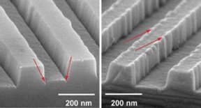
The new approach, described in the June 20 Nature, would do away with the stencils and the optical paraphernalia that goes with them. Stephen Y. Chou, Chris Keimel, and Jian Gu have instead sculpted the silicon surface by pressing a sturdy mold of etched quartz against it. An ultraviolet laser shoots through the clear quartz into the underlying silicon, briefly melting the surface. The mold sinks slightly, embossing its pattern as the silicon resolidifies.
In today’s chip-manufacturing plants, $10 million machines called steppers shift precisely from one position to the next across a silicon wafer, pausing briefly at each chip location to project the pattern for one level of a circuit-to-be (SN: 7/21/01, p. 38: Available to subscribers at Optics oddity challenges microchip makers). Chou envisions a faster method in which an array of identical molds presses into a wafer all at once to imprint one layer onto hundreds or thousands of chips.
“This method is a genuinely innovative and unexpected way of making microstructures in silicon,” comments George M. Whitesides of Harvard University. It should work for other semiconductors and metals, too, adds Chou.
Although making the molds themselves requires the most-advanced techniques of patterning and etching, those steps would be required for only a single master per layer, Chou explains. “Once you have your first mold, you’re home free,” he says.
The new technique also shows promise for making circuitry with much smaller components than are currently feasible. Today’s commercial chip-making methods can carve surface structures as small as 65 nanometers across, whereas the new imprinting method has generated features in silicon less than a sixth that size.
“On the grounds of cost, speed and resolution, [the new method] may displace optical technology as the preferred manufacturing technology for fashioning silicon chips,” predicts R. Fabian Pease of Stanford University in a commentary in the same issue of Nature. If so, he adds, the industry can probably maintain its breathless pace of miniaturization for another 20 years.